February 11, 2020
Mechanism of electrostatic breakdown
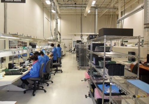
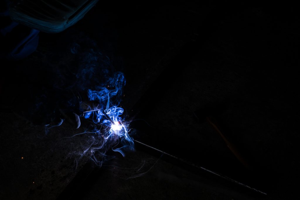
Electrostatic discharge and their damages (from electrostatic breakdown) are a major problem for industrial manufacturing processes. Not only it can damage the production and machines, it also endangers workers.
Mechanism
Electrostatic breakdown is a phenomenon in which electronic components such as integrated circuits (ICs) are destroyed by static electricity. Damages by static electricity occur due to high voltage temporarily flowing through the ICs coming from an electrostatic discharge.
When ESD happens, a thin film (insulating layer) such as highly insulating silicon oxide is broken on the ICs. Therefore, the circuit inside is destroyed.
In recent years, electronic components have become lighter and smaller. Therefore, their sensitivity to static electricity has also increased.
In particular, metal–oxide–semiconductor (MOS) lose their function as semiconductors when only a voltage of about 80 to 100 V is applied.
Electrostatic shock
Electrostatic shocks can be detrimental to delicate semiconductor devices, even at relatively low voltages. To give an indication, humans can feel the pain from an electrostatic shock when the voltage is only about 3 kV. This gives you an idea of how small the voltage is and yet still it can damage the production of semiconductors.
Nowadays, as semiconductor devices become finer and more complex circuits, the wiring spacing (the size of the elements themselves) also becomes smaller. So their electrostatic resistance becomes lower. In some cases, such as when the oxide film is incomplete, it can even be destroyed at lower voltages. That is why more sophisticated measures for managing static electricity are required from manufacturers.
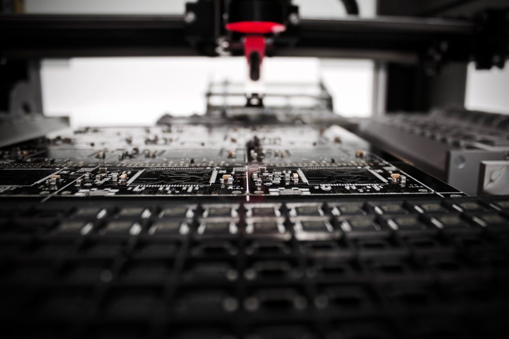
Semiconductors
Here are some examples of common damages due to electrostatic breakdown from electrostatic discharge, related to the semiconductors:
- When peeling off wafer rack: due to exfoliation charging that occurs during wafer transfer and removal from the wafer rack.
- When peeling the protective film from the substrate: electrification occurs when a protective film is peeled from a liquid crystal glass substrate.
- Sheet peeling during chip mounting: due to peeling electrification that occurs when chips are picked from a wafer sheet.
Charged objects that cause electrostatic breakdown
Workers, equipment, and the semiconductor element itself can be considered as charged objects that cause electrostatic breakdown.
In order to implement the correct solution to prevent ESD, there are 3 existing ESD test models:
1.The Human Body Model (HBM): When a charged worker carelessly brings a finger close to a semiconductor element. (Because humans move around and perform various tasks, they are extremely easily charged.)
2. The Machine Model (MM): The device is charged when the device comes into contact with the charged conductor and the device is grounded, causing electrostatic breakdown.
3. The Charge Device Model (CDM): The circuit of a semiconductor device is charged, and is discharged when a terminal of the device approaches a nearby conductor. This causes electrostatic breakdown in an internal circuit.
1. Human body charging model (HBM)
The device is charged due to discharge when an electrostatically charged person touches the lead of the device. And when the device is grounded, a discharge current flows through the circuit, causing electrostatic breakdown.
The amount of charge released from the charged human body is large, and the discharge energy is extremely large compared to the case of an insulator.
2. Machine model (MM)
If the electrostatically charged object is a device, it is called a “machine model”.
If the equipment used in the manufacturing process is not grounded, the conductors will also become charged. Then, when the charged body touches the external terminal of the semiconductor device, electric current penetrates through the device and causes electrostatic breakdown.
3. Charged device model (CDM)
Even if human body models and machine models are adequately protected against static electricity, there is a possibility that ESD induced destruction will occur during the production and assembly of semiconductor devices.
This is due to electrostatic discharge damage when the device itself is charged, and is called “device charging model”.
In this discharge model, the device itself is charged by friction on the surface of the semiconductor device. As a result, conductors such as circuits and leads cause electrostatic induction by an external electric field. In this state, if the lead is grounded, the internal electric field will change abruptly and the discharge current will flow, causing electrostatic breakdown.
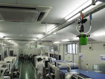
How can IKEUCHI help?
As mentioned, electronics components are becoming smaller and smaller. Therefore, more sophisticated measures are required to help manufacturers preventing electrostatic breakdown damages on their production.
We have researched the optimal solution to prevent electrostatic discharge (ESD), by adding humidity in a working environment. Our non-wetting Dry Fog humidifier offers the adequate solution for sensitive working stations.